Communication between SoC and FPGA
This document describes how FPGA and SoC communicate with each other in TwPM project for NEORV32. State presented here is valid for release v0.2.0 of top module.
Memory map
| Address | Size | Name | Access |
|---|---|---|---|
| 0xF0000000 | 4B | STATUS | RO |
| 0xF0000004 | 4B | OP_TYPE | RO |
| 0xF0000008 | 4B | LOCALITY | RO |
| 0xF000000C | 4B | BUF_SIZE | RO |
| 0xF0000040 | 4B | COMPLETE | WO |
| 0xF0000800 | 2KiB | FPGA_RAM | RW |
Reads from invalid addresses in 0xF0000000-0xF0000FFF range return 0xBADFABAC
(BAD FABric ACcess), writes are dropped. Most values are valid only if exec
bit in STATUS register is set.
Registers
Reserved bits are read as 0. They may change in the future.
STATUS

execindicates that MCU is expected to act upon request sent from FPGA, specified inOP_TYPEregister. Interrupt is generated when this signal gets set by FPGA.abortis set when PC aborts command currently being executed by TPM.completeis a signal sent towards FPGA by writing toCOMPLETEregister. The signal is active for a few cycles after write to that register, after that is should be automatically set back to 0.
OP_TYPE
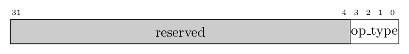
op_typeis a type of operation expected from MCU. 0 is used as a default value to which this register returns aftercompletesignal is acknowledged by FPGA, code should treat this value as error because no valid path produces it when requesting interaction from MCU. 0xC is reserved as it may be part of 0xBADFABAC magic value. This register is only valid ifexecis set.
| op_type | Operation |
|---|---|
| 0x0 | No operation |
| 0x1 | Execute TPM2 command located in FPGA_RAM |
| 0xC | Illegal operation type |
| other | Reserved for future use |
LOCALITY

localityspecifies the locality at which the current operation was initiated. Value 0xF is used when no locality was active at that point. This field is only valid ifexecis set.
BUF_SIZE

buf_sizespecifies size (in bytes) of data available in FPGA RAM, which is usually a TPM2 command. This field is only valid ifexecis set. TPM stack is not expected to write size of response to this field, it is deduced from response's payload.
COMPLETE
Any write to this register triggers complete signal to be sent to FPGA. Reads
from this register aren't implemented, meaning that 0xBADFABAC is returned.
FPGA RAM
This region behaves like RAM if exec is set. Its content depends on op_type,
which in most cases will be TPM2 command. Response is written by MCU to this
buffer, starting from offset 0, overwriting the command.
When exec is not set, data read from this region is invalid and writes are
dropped.
Interrupts
TwPM needs to communicate from FPGA towards SoC when there is an operation to be
performed by TPM stack. This is done through mext_irq_i, which is responsible
for signaling Machine external interrupt (MEI). This signal is level-triggered
and high-active. MEI has a dedicated value in mcause, shared between all
external interrupts. The exact reason has to be obtained in a platform-specific
way; in case of TwPM it can be read from STATUS register, however, as of now
only exec generates an interrupt so this check is redundant.
The interrupt signal remains active until SoC signals completion by performing
a write to COMPLETE register. For this reason, the IRQ must be masked when TPM
command is being executed outside of interrupt service routine (ISR).